(Click for bigger pictures)
The PDP-4/X is a reimplementation of one of Digital Equipment Corporation's 18-bit computers, with 32K words of memory, an extended memory control, a line frequency clock, an interface to an RS-232 terminal, and an interface to an IDE disk, which I built just for fun.
As it's name implies, the model for the PDP-4/X is the PDP-4, which was the oldest and simplest of the bulk of Digital Equipment Corporation's 18-bit computers (the PDP-1 is older, but isn't really part of the PDP-4/-7/-9/-15 family; the reimplementation of the PDP-1 is another project).
The PDP-4/X has 32K words of memory and an extended memory control, and although the PDP-4 documents talk about a 32K PDP-4, no description of the extended memory control seems to have survived (and Gordon Bell isn't sure it even existed), and so I implemented the PDP-7 extended memory control, with a couple of small modifications whicb will be explained in the software section.
The PDP-4/X has an extended arithmetic element (EAE), mainly so that PDP-9 FORTRAN would run. Once again, although the PDP-4 documents talk about an extended arithmetic element, no description of it seems to have survived, and so I implemented the PDP-7 extended arithmetic element.
The PDP-4/X has a terminal interface capable of sending and receiving 8-bit characters in full-duplex mode. The interface could be used to send and receive 5-bit (BAUDOUT) characters, but none of available software, either written from scratch for the PDP-4/X, or ported from the PDP-9/PDP-15, supports a BAUDOUT terminal. The PDP-4/X also has a simple disk interface, which communicates with IDE disks using programmed I/O operations.
The PDP-4/X is described in detail in the PDP-4/X System Reference Manual.
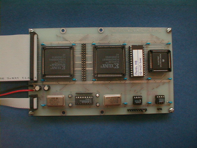
The CPU is implemented with a XILINX XC4010E (5.0V, 20x20 CLBS) field programmable gate array (FPGA), which contains the basic processor, the memory extension control, the extended arithmetic element, half of the line frequency clock (the part the deals with incrementing location 00007), and the logic which assists the front panel program.
A single 64Kx18 SRAM (Motorola MCM67A618A) implements the 32Kx18 normal memory and the 32Kx18 front panel memory. The CPU drives the address and control signals to the SRAM.
The front panel program is stored in a 32Kx8 EPROM (27C256), the contents of which are copied into the low 8K words of front panel memory at reset time. The EPROM data is actually six bits wide; the CPU reads three 6-bit values from the EPROM, packs them into an 18-bit word, and writes the word into memory.
The IOU is implemented with a XILINX XCS05 (SPARTAN, 5.0V, 10x10 CLBS) FPGA, which contains the other half of the line frequency clock (the 60 Hz clock, the enable bits, and the flags), the terminal interface, and the IDE disk interface. The terminal interface watches for framing errors, and when one is detected, a HALT REQUEST is sent to the CPU, on the assumption that the framing error was caused by the user generating a BREAK.
The CPU sends IOT instructions to the IOU over the data bus.
Here's a block diagram of the CPU.

The CPU has two major sections. The 15-bit wide address section (which includes the PC and MA registers) generates and sequences all of the addresses which are supplied to the memory. The 18-bit wide data section (which includes the MDI, MDO, AC, LINK, MQ, SC, and SR registers) does all the computation.
The address section consists of the MA and PC registers, connected in a ring by conditional increment logic. The increment betweem the MA register and the PC register is used to compute sequential addresses during normal program execution and to compute the "+1" which happens during JMS. The increment between the PC register and the MA register is used by skips. A multiplexor at the front of the MA register selects between the output of the skip increment, the output of the data section (which supplies addresses for memory reference instructions), and the constant 20 (which is needed by CAL). The other two constant addresses (0 for interrupts, 7 for the clock) are handled differently; "JMS 0" and "ISZ 7" instructions are forced into the MDI register for interrupts and clock ticks.
The heart of the data section is the ALU and ROTATE logic. The ALU is an 18-bit ripple carry adder which can also compute logical OR, and the ROTATE is a bunch of 5-input multiplexors which can rotate left or right by one or two bit positions.. One side of the ALU is fed by the AMUX multiplexor and the ASEL box. The AMUX selects between MDI, SR, MQ, or SC. The ASEL selects between 0, the AMUX, the ones complement of the AMUX, the AUMX and'ed with AC, and the AMUX xnor'ed with AC. The AMUX xnor'ed with AC function is used both by XOR (with the addition of a ones-complement) and by SAD (which can implement the equality check with an increment in the ALU and a carry check). The other side of the ALU is fed by the BSEL box, which selects between 0, 777777, AC, or the ones-complement of AC.
Memory data flows into the data section through the MDI register, and flows out of the data section through the MDO register. A multiplexor at the input of the MDO register can select the PC for JMS (this multiplexor also puts the LINK and the extend mode flag in the correct locations in the saved PC word).
The control is based on a sequence of major cycles, each of which is a sequence of 4 ticks of the 8 MHz system clock. In general a memory or I/O read happens in ticks 0 and 1 of a major cycle, and a memory or I/O write happens in ticks 2 and 3 of a major cycle. The timing is arranged so that data read in ticks 0 and 1 can be passed through the data path and written in ticks 2 and 3, which makes things like the ISZ instruction and auto-indexing fairly straightforward. The timing of the external strobes guarantees a half-tick between read data and write data, and a half-tick of write hold.

The major cycles are similar to those of a real PDP-4. The F major cycle reads instructions. The D major cycle reads indirect addresses, and performs auto-indexing. The E major cycle executes memory reference instructions. Operate instructions, and IOT instructions which manipulate the state of the CPU itself (device 00 and device 77), are executed in tick 2 of the F major cycle (this is possible because the soft switch register is inside the CPU. The S major cycle does setup for EAE instructions, and the A major cycle, repeated as many times as the SC counter demands, does arithmetic for those instructions.
IOT instructions which manipulate I/O devices are tricky because the CPU cannot look at the instruction and determine its function. These instructions are executed by an I major state. During the read portion of the I major state the device sends two command bits to the CPU telling it how the instruction should be executed (the command bits are an ISKP bit which says that the next instruction should be skipped, an IORA bit which says that the data being supplied during the read portion of the I major state should be combined with the AC register with an inclusive-or operation). During the write portion of the I major state the value of the AC register is made available to the device, which writes it into an internal register if it desires. The command bits are low-true and pulled up by resistors, so that if the device is unknown, the command bits are all false, which makes the IOT do nothing.
The I major cycle is unique in that it can be externally stretched to allow for slow I/O devices. Clock ticks can be added between tick 0 and 1 (stretching the read portion of the cycle) or between tick 2 and 3 (stretching the write portion of the cycle). The stretch signal is low true and pulled up by a resistor, so the default is to run at full speed.
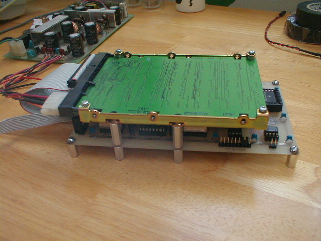
I built the PDP-4/X on a small printed circuit board. Note that unlike my earlier PDP-8/X design, the mounting holes in the printed circuit board have been made to line up with the mounting holes on the IDE disk drive, which allows for a very compact assembly using various lengths of off-the-shelf spacers.
Not much software for the 18-bit systems survives.
The first software I ran on the PDP-4/X emulator and hardware was the front panel program (PANEL.008), immediately followed by the PDP-4 basic instruction test (it doesn't test much, but it's authentic), some custom tests (the teletype interface, the disk interface, the EAE), and the three subsections of the PDP-15 basic instruction tests. Getting the PDP-15 basic instruction tests to pass required that that the tests be reverse-assembled, edited a little (to remove code which could only pass on a PDP-15, like the tests for the IAC and BSW operate micro-operations, and the tests for operation in page mode), and reassembled.
Once this was all working I ran a version of BASIC (BASIC.006) which I wrote from scratch. History buffs whill observe that the PDP-4 and BASIC were youngsters at the same time; the first PDP-4 shipped in July 1962, and Kemeny and Kurtz ran the first BASIC program on the GE-225 in May 1964.
I then decided that I would try and get a version of the PDP-9/PDP-15 advanced system software running on the PDP-4/X. This seemed like it would be possible, since images of the system DECtapes, and some sources, exist on several websites, and the PDP-4/X is very similar to the PDP-9/PDP-15. On the other hand, much of the documentation had not survived, and the documentation which does survive made it clear that this kind of adaptation was going to be difficult. I did, however, succeed; the PDP-4/X runs the PDP-9/PDP-15 advanced system software well enough to be able to compile and run programs in both MACRO and FORTRAN. The PDP-4/X is very similar to the PDP-9/PDP-15, but two details of the extended memory control needed to be changed to make like the PDP-9/PDP-15; autoindexing in any memory field references autoindex locations in field 0, and the extended memory interrupt restore was changed to function more like the DBR instruction.
There were three parts to getting the PDP-9/PDP-15 advanced system software running on the PDP-4/X.
The first was reverse-engineering the DECtape bootstrap and creating an IDE bootstrap (DTLDR.003) which would treat the front of the disk as eight 576-block DECtape images. This turned out to me much harder than it first appeared to be, because the bootstrap is also used by the system as a disk handler, so a large number of absolute addresses need to be preserved, and it has to fit in locations 77637 through 77777.
The second was writing two new device handlers. The first handler (DTSYS.001) only needs to be able to handle IOPS input modes from a single file. This handler is actually part of the system loader, is assembled at a known location (73400 in a 32K system), and lives in dedicated blocks (56, 57, 60) on the system disk. The second handler (DTHAN.001) needs to be able to handler multiple files, all IOPS modes, and all TRAN modes (the TRAN modes are needed by PIP, which has commands to list and zero the DECtape direcory). This handler lives in the system library (LIBR.BIN), and is loaded by the system loader when necessary. Neither of these handlers were well documented, and a lot of details were determined by extracting examples from the system library, and looking hard at the reverse-assembler's output.
The third was putting things together. A new 32K DECtape image was generated by runing SGEN under Bob Supnik's SIMH PDP-9/PDP-15 emulator. The system library file was extracted from this DECtape image, and a new system library file, containing the new DTA handler, was generated using a cross assembler and library editor. A new disk image was generated using a cross system builder, which combined the DECtape image, the new DTC handler, and a lot of patches, to make a new 32K disk image (the cross system builder was also responsible for figuring out what blocks on the DECtape would have been written in the reverse direction, and reformatting the data in the block, because the disk has no notion of reading and/or writing in the reverse direction). The system was debugged on the simulator, at which point the boottable disk image was copied over the serial line and written onto the disk.
Updated: January 08, 2005